- 您现在的位置:买卖IC网 > Sheet目录328 > IDT7006L55G (IDT, Integrated Device Technology Inc)IC SRAM 128KBIT 55NS 68PGA
IDT7006S/L
High-Speed 16K x 8 Dual-Port Static RAM
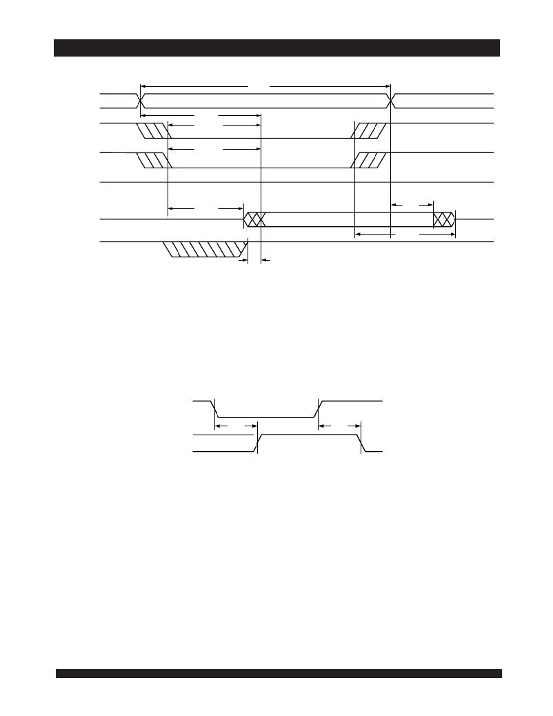
Waveform of Read Cycles (5)
ADDR
t AA (4)
t RC
Military, Industrial and Commercial Temperature Ranges
CE
t ACE (4)
t AOE (4)
OE
R/ W
VALID DATA
DATA OUT
t LZ (1)
(4)
t OH
t HZ (2)
BUSY OUT
t BDD (3,4)
2739 drw 07
NOTES:
1. Timing depends on which signal is asserted last, OE or CE .
2. Timing depends on which signal is de-asserted first CE or OE .
3. t BDD delay is required only in cases where the opposite port is completing a write operation to the same address location. For simultaneous read operations BUSY
has no relation to valid output data.
4. Start of valid data depends on which timing becomes effective last t AOE , t ACE , t AA or t BDD .
5. SEM = V IH .
Timing of Power-Up Power-Down
CE
I CC
I SB
t PU
8
t PD
2739 drw 08
,
发布紧急采购,3分钟左右您将得到回复。
相关PDF资料
IDT7007L20G
IC SRAM 256KBIT 20NS 68PGA
IDT7008L25G
IC SRAM 512KBIT 25NS 84PGA
IDT7009L20PFI
IC SRAM 1MBIT 20NS 100TQFP
IDT70125L25JG
IC SRAM 18KBIT 25NS 52PLCC
IDT7014S12JG
IC SRAM 36KBIT 12NS 52PLCC
IDT7015L35G
IC SRAM 72KBIT 35NS 68PGA
IDT7016L35G
IC SRAM 144KBIT 35NS 68PGA
IDT7019L20PFI
IC SRAM 1.125MBIT 20NS 100TQFP
相关代理商/技术参数
IdT7006L55GB
制造商:Integrated Device Technology Inc 功能描述:IC SRAM 128KBIT 55NS 68PGA
IDT7006L55J
功能描述:IC SRAM 128KBIT 55NS 68PLCC RoHS:否 类别:集成电路 (IC) >> 存储器 系列:- 标准包装:45 系列:- 格式 - 存储器:RAM 存储器类型:SRAM - 双端口,异步 存储容量:128K(8K x 16) 速度:15ns 接口:并联 电源电压:3 V ~ 3.6 V 工作温度:0°C ~ 70°C 封装/外壳:100-LQFP 供应商设备封装:100-TQFP(14x14) 包装:托盘 其它名称:70V25S15PF
IDT7006L55J8
功能描述:IC SRAM 128KBIT 55NS 68PLCC RoHS:否 类别:集成电路 (IC) >> 存储器 系列:- 标准包装:45 系列:- 格式 - 存储器:RAM 存储器类型:SRAM - 双端口,异步 存储容量:128K(8K x 16) 速度:15ns 接口:并联 电源电压:3 V ~ 3.6 V 工作温度:0°C ~ 70°C 封装/外壳:100-LQFP 供应商设备封装:100-TQFP(14x14) 包装:托盘 其它名称:70V25S15PF
IDT7006L55JB
制造商:IDT 制造商全称:Integrated Device Technology 功能描述:HIGH-SPEED 16K x 8 DUAL-PORT STATIC RAM
IDT7006L55L68
制造商:未知厂家 制造商全称:未知厂家 功能描述:x8 Dual-Port SRAM
IDT7006L55L68B
制造商:未知厂家 制造商全称:未知厂家 功能描述:x8 Dual-Port SRAM
IDT7006L55PF
功能描述:IC SRAM 128KBIT 55NS 64TQFP RoHS:否 类别:集成电路 (IC) >> 存储器 系列:- 标准包装:45 系列:- 格式 - 存储器:RAM 存储器类型:SRAM - 双端口,异步 存储容量:128K(8K x 16) 速度:15ns 接口:并联 电源电压:3 V ~ 3.6 V 工作温度:0°C ~ 70°C 封装/外壳:100-LQFP 供应商设备封装:100-TQFP(14x14) 包装:托盘 其它名称:70V25S15PF
IDT7006L55PF8
功能描述:IC SRAM 128KBIT 55NS 64TQFP RoHS:否 类别:集成电路 (IC) >> 存储器 系列:- 标准包装:45 系列:- 格式 - 存储器:RAM 存储器类型:SRAM - 双端口,异步 存储容量:128K(8K x 16) 速度:15ns 接口:并联 电源电压:3 V ~ 3.6 V 工作温度:0°C ~ 70°C 封装/外壳:100-LQFP 供应商设备封装:100-TQFP(14x14) 包装:托盘 其它名称:70V25S15PF
